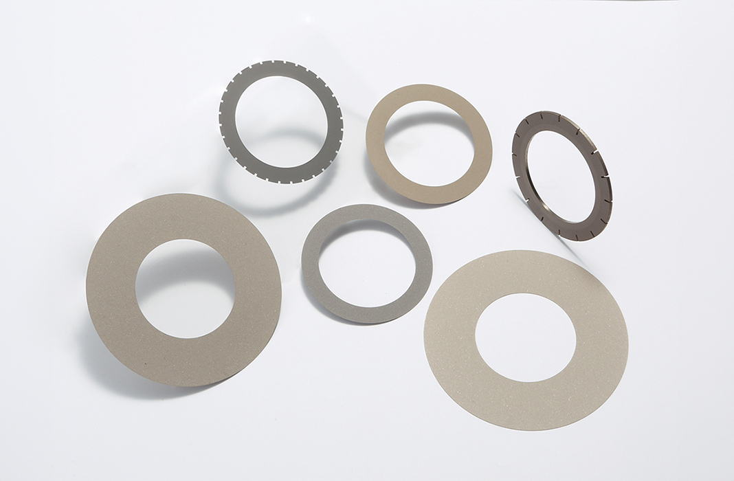
Dicing Blade
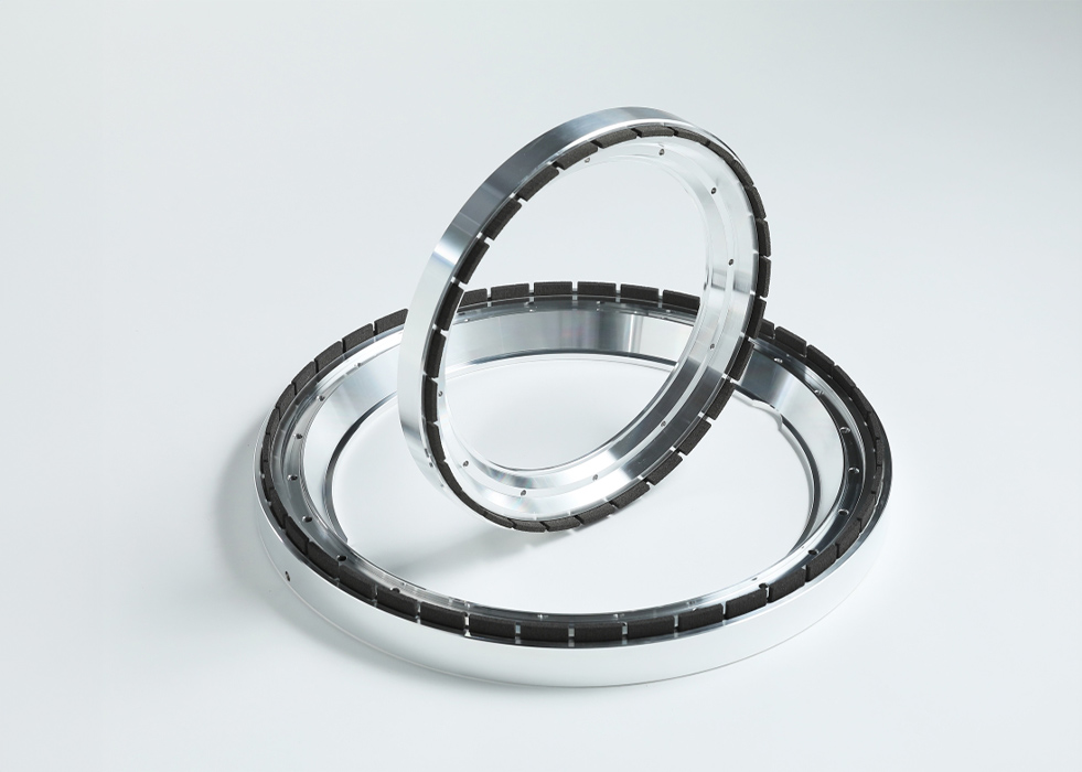
Diamond wheel for grinding SiC surfaces "M-cloud"
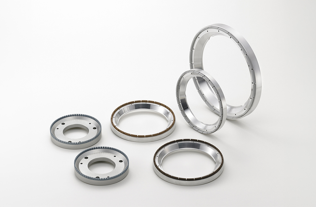
This is a diamond wheel for surface grinding of various wafers such as semiconductor materials and electronic device materials. We provide the most suitable wheels for each material. It minimizes machining damage, improves machining efficiency, and contributes to the reduction of machining costs. It can be customized according to the customer's needs.
Provide various wheels for each applications
Modify wheel specifications upon request of customers
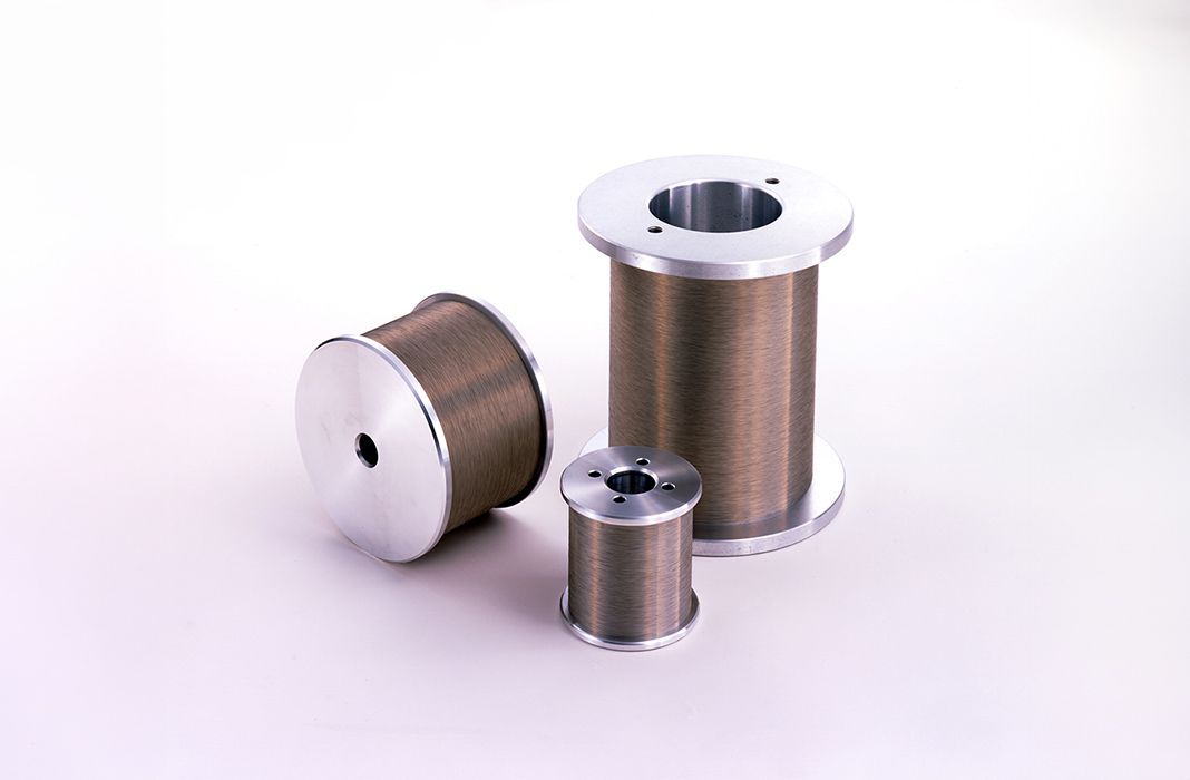
Resin Wheels
Recommended for Silicon Wafer, Heat sink substrate, and Encapsulation materials
Vitrified wheels
Recommended for almost all "electronic components and semiconductor's substrates and materials
Metal wheel
Recommended for Support substrate, Heat sink substrate, Sapphire, and Encapsulation materials
Other optimal specifications are available upon request.
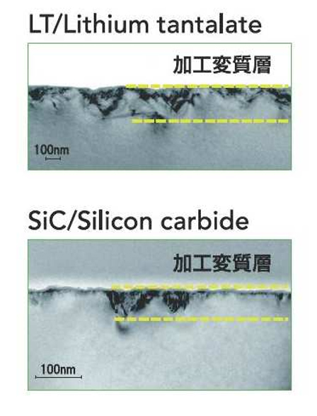
Comparison of surface roughness and damage depth after grinding various semiconductor substrate materials with a high number wheel
| Work material | Mesh size | Bond Type | Surface roughness | Damage depth |
|---|---|---|---|---|
| Φ12inch-Si | #30000 | Vitrified | 1~2nm | ≦100nm |
| Φ6inch-LT | #8000 | Vitrified | 3~5nm | ≦250nm |
| Φ6inch-LN | #8000 | Vitrified | 2~4nm | ≦350nm |
| Φ6inch-SiC | #30000 | Vitrified | ≦1nm | ≦100nm |
| Φ2inch-GaN | #30000 | Vitrified | ≦1nm | ≦450nm |
EMC and Cu
No drag, etc. even with high Cu occupancy.
Less step difference between EMC and Cu.